01
Application structure
Package substrates, HDI/SLP, flexible circuits, thermally conductive insulation and functional coatings require different material forms and evaluation priorities.
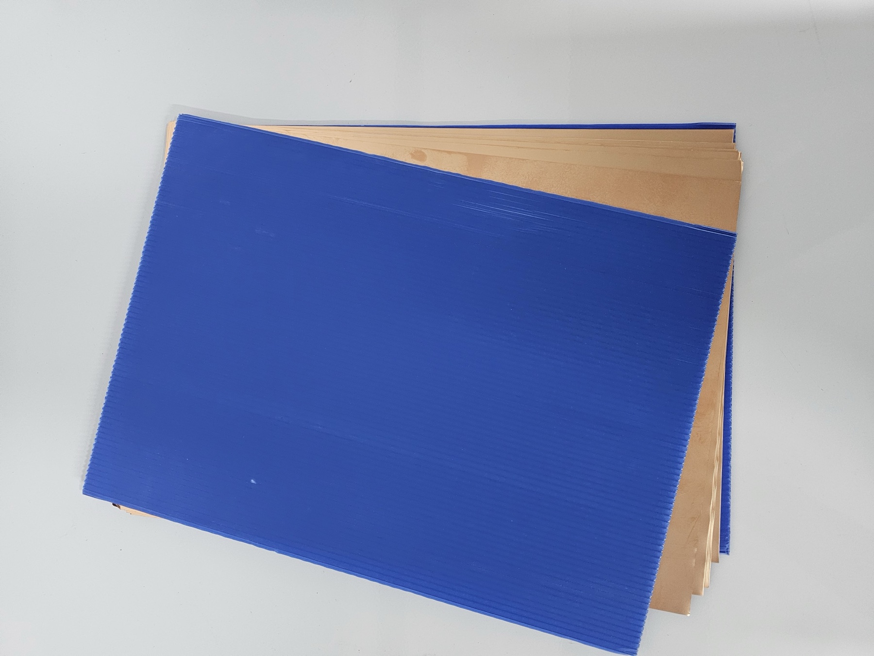
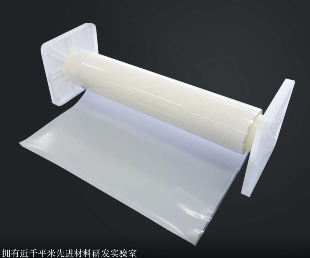
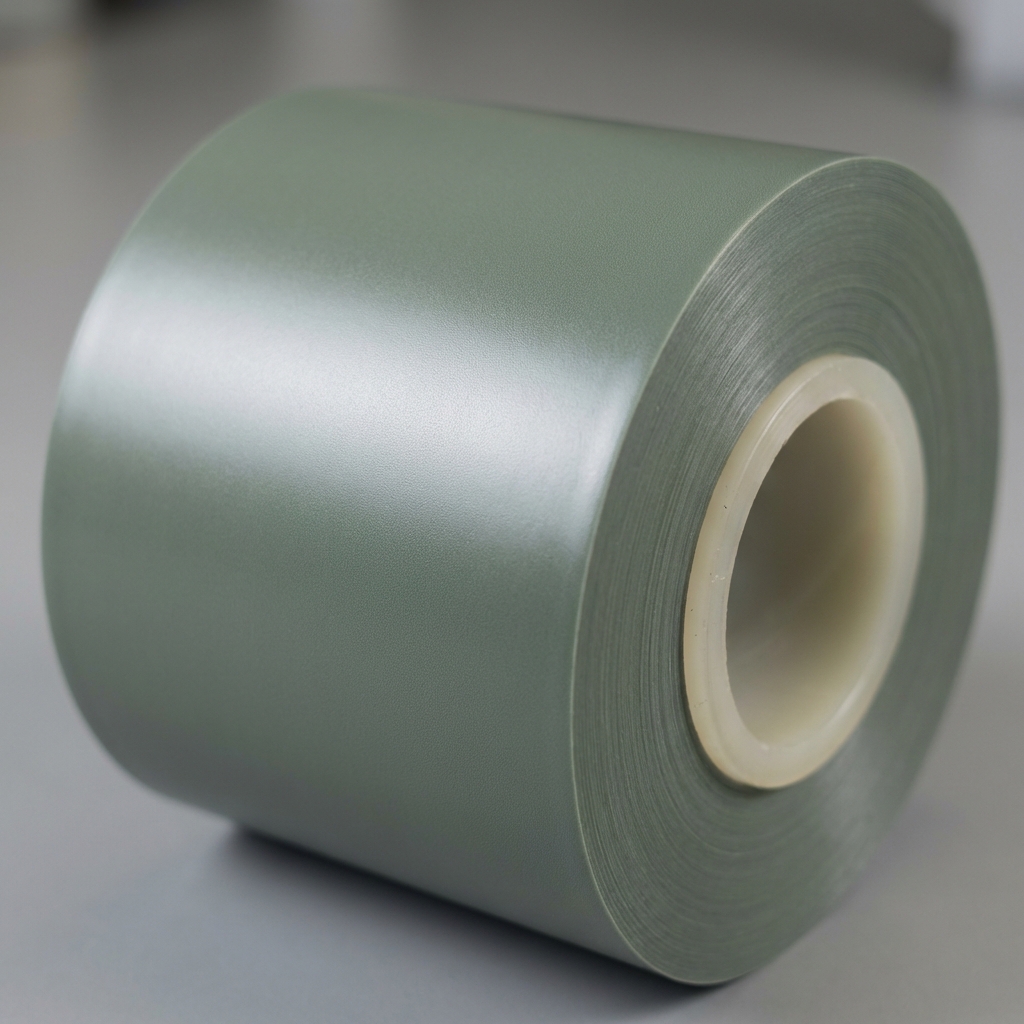
The portfolio covers package substrate films, resin coated copper, flexible composite films, specialty functional films and electronic pastes. ABF-type build-up materials are one branch within the package-substrate route.
Yipengchunhui supports material selection through application structure, key data, process windows and sample validation.
Package substrates, HDI/SLP, flexible circuits, thermally conductive insulation and functional coatings require different material forms and evaluation priorities.
Thickness, Tg, Df, CTE, thermal conductivity and adhesion define the initial material boundary.
Evaluate lamination, laser drilling, plating, reflow and reliability conditions together.
Validate the material against the customer's real stack-up, target process and reliability requirements.
AEM is built on an IC composite materials platform covering package substrates, PCB, SLP, embedded structures, RDL, molding, die bonding and functional paste applications.
SAP, microvias, fine lines, high Tg and low CTE.
Compatible with horizontal desmear and conventional lamination.
For power devices, passive embedding and thin dielectric layers.
For FOPLP, WLP, 2.5D RDL layers and fine-line build-up.
Low CTE, thermal insulation and thick-film build-up for MIS, ETS and FOPLP.
High adhesion, low moisture uptake and flexible cured film.
Screen printing or brushing for insulation protection and functional paste layers.
For bonding, insulation protection and long-term reliability.
Films, copper-clad forms, flexible composites and pastes are developed around real process introduction, balancing material performance, process windows and reliability.
 01
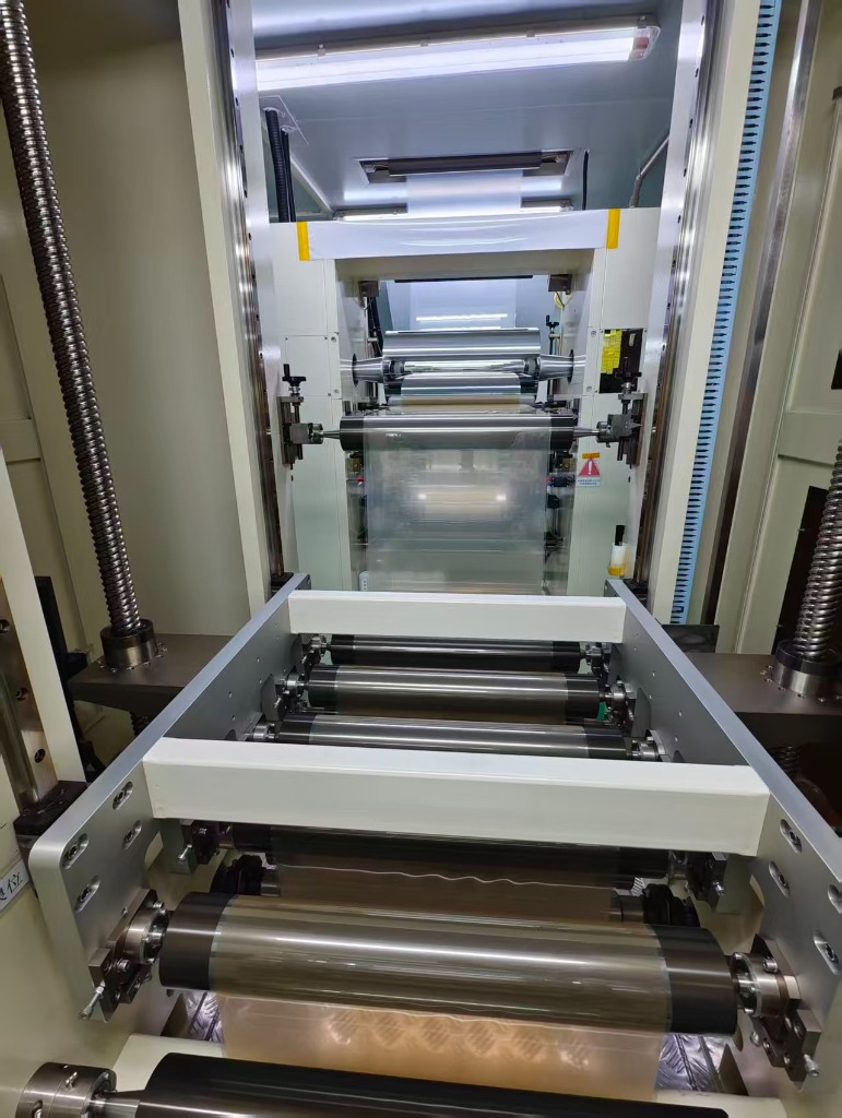
01Material design starts from resin chemistry, filler dispersion and target dielectric or thermomechanical behavior.
 02
02Dispersion, coating, drying, winding and paste solid content control stabilize appearance, thickness and batch consistency.
 03
03Package substrates, HDI, flexible circuits, thermal-management structures and functional coatings correspond to different material series.
For FC-BGA, Chiplet and AI server package substrates.
For build-up insulation, fine-line formation and reliable package substrate stack-ups.
Focus on low loss, low CTE, Tg, thickness uniformity and SAP/semi-additive process windows.
Evaluate target line/space, dielectric thickness, laser drilling, copper plating and reflow reliability together.
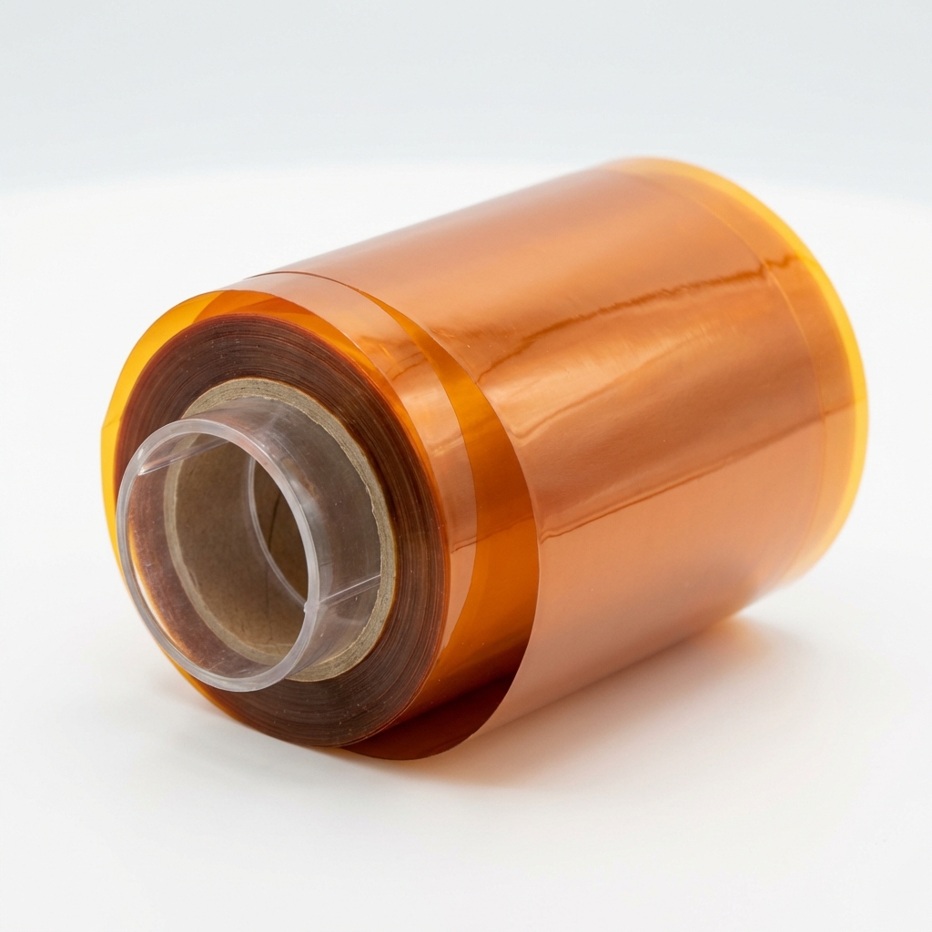
Standard F-series film for package substrates, balancing insulation reliability and process adaptability.
Low-CTE grade for package substrate designs that require improved dimensional stability.
Low-loss, high-Tg film for high-speed interconnect and advanced package substrate evaluation.
Ultra-low-loss grade for demanding AI server, 5G/6G and high-bandwidth interconnect applications.
Thermoset insulating film for SAP package substrates with L/S down to 25/25 μm.
For HDI, SLP, copper filling, embedded devices and conventional lamination processes.
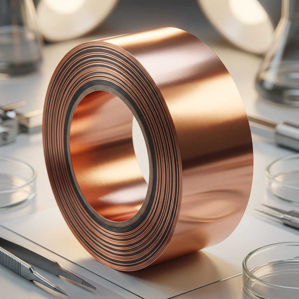
For HDI, SLP and build-up structures that need copper-clad film introduction.
Focus on copper foil compatibility, filling behavior, lamination window, dimensional stability and high-frequency loss.
Clarify copper foil type, lamination conditions, via structure, filling depth and surface treatment requirements.
Standard RCC grade for HDI and rigid PCB processes requiring filling capability and insulation reliability.
RCC grade with improved dimensional stability and lower dielectric loss for advanced HDI structures.
High-frequency RCC grade combining low loss, heat resistance and mechanical stability.
Ultra-low-loss RCC grade for high-end copper foil systems and fine-line applications.
For FPC, foldable displays, wearables and dynamic bending structures.
For flexible circuits, wearables and dynamic bending insulation or bonding structures.
Focus on elongation, peel strength, heat resistance, moisture uptake and resin flow control.
Evaluate bending radius, bending cycles, copper foil structure, coverlay process and soldering temperature.
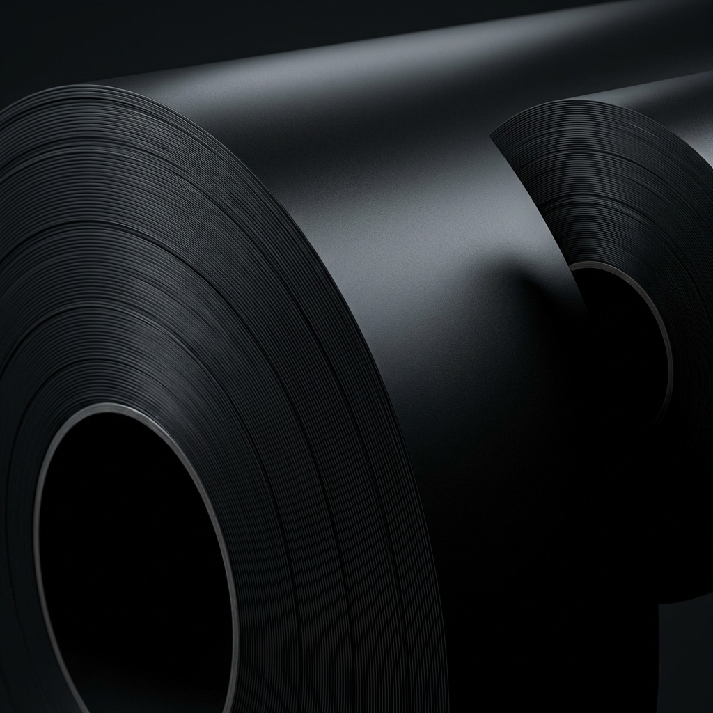
High-flexibility film for FPC and dynamic bending applications.
Balanced flexible grade for structures that require both flexibility and heat resistance.
Heat-resistant flexible film for FPC structures with higher process temperature requirements.
Thermoset flexible composite film for reliable bonding, insulation protection and cured-film flexibility.
PI-release flexible composite film for circuit insulation protection, functional layer bonding and battery module bonding.
For PLP, low-warpage structures and thermally conductive insulation.
For panel-level packaging, power devices and insulation layers requiring low CTE or thermal conductivity.
Focus on CTE, modulus, thermal conductivity, dielectric loss and large-area warpage control.
Evaluate chip size, package structure, thermal path, reflow conditions and reliability targets together.
For screen printing, insulation protection, conductive or insulating functional layers and bonding applications.
For resistor protection, functional coatings, conductive or insulating paste layers and composite bonding scenarios.
Focus on solid content, adhesion, coating window, chemical resistance, low moisture uptake and long-term reliability.
Evaluate printing or brushing method, drying time, curing profile, substrate interface and environmental reliability together.